Quartus SOPC Project
Build a SOPC architecture around the Nios II CPU
Create a new Quartus project
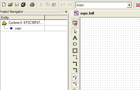
Start by building a blank Quartus project
Start the SOPC Builder
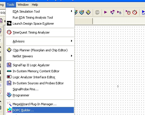
Start the SOPC Builder tool from Tools -> Sopc Builder menu as shown in the figure
Start by entering a name for the new system
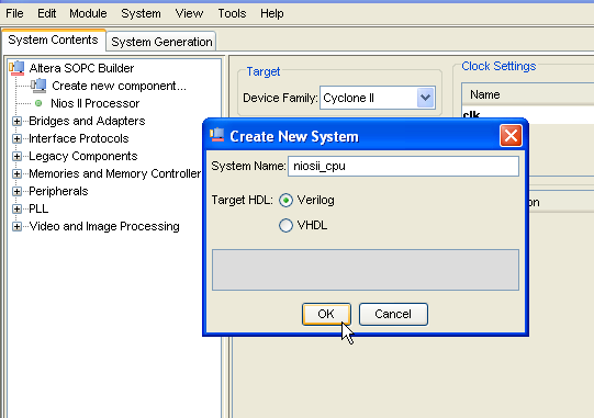
Select also the prefered HDL (Verilog or VHDL) for defining the system
Add the CPU component
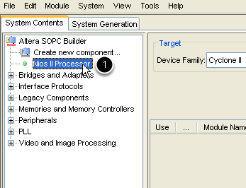
Add the Nios II processor by double clicking its corresponding element in the System Contents tab.
Configure the CPU
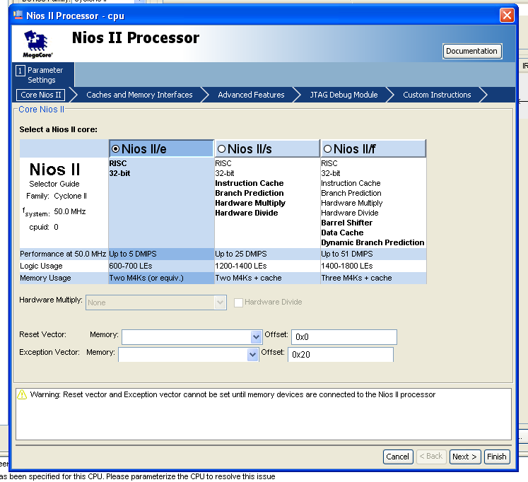
In the following 4 steps, the Nios II CPU will be configured in order to serve the project's objectives. For a simple project, aiming to controll the Altera DE2's LCD and to intercept the characters sent by a PS/2 keyboard connected to the DE2 board, we will select a Nios II/e CPU (the one with the fewer features) in the first step (presented in the image above), jumping over the second step, selecting no cpu_resetrequest in the third step and selecting No Debugger option on the final step.
Note: After inserting the memory components (both for instruction and data), The Reset vector and the Exception vector (seen in this figure) as well as the Break vector (available in the forth step of CPU's configuration) need to be set.
Configure the CPU cont'd
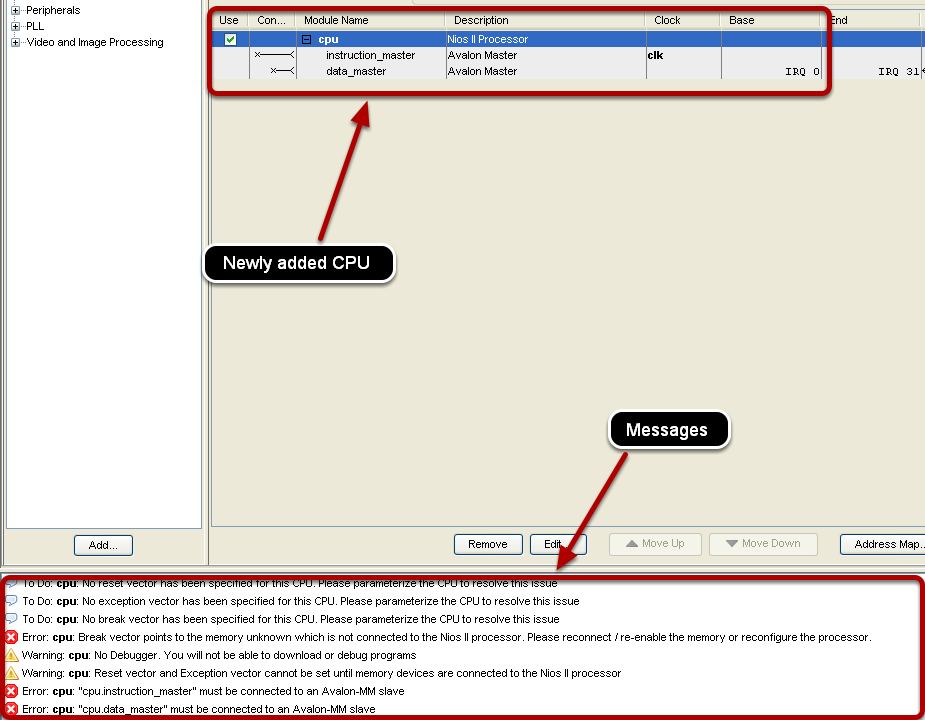
The system's structure, as seen in the System Contents tab will be updated including the new CPU component as shown in the image. The new CPU have two master subcomponent: one which will need to comunicate with a slave attached to the program (instruction) memory, named instruction_master and one for comunnicating with a slave attached to the data memory, named data_master. The master-slave pairs are managed by the Avalon component of a System designed with Quartus's SOPC Builder. More informations can be found here.
Note: The message portion of the System Contens tab display all the errors as well as configurations required to be made in order for thedefined architecture to be generated. Pay attention to these messages and resolve any of them requiring a specific action.
Add a memory component for the instructions
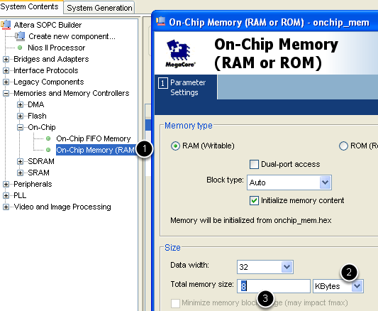
In the components tree of the System Contents tab, add a new "On-chip Memory (RAM or ROM)" component by double clicking it as shown in the figure. We will configure the module to be a RAM module (as oposed to a read only memory component) having a capacity of 8KB. This is accomplished by modiying the configuration indicated at the point marked with 2 and 3. Press the Finish button afterward.
Configure the memory component for instructions
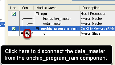
By default, the newly created module is attacjed a slave Avalon sub-component and connected to both the instruction and the data master of the CPU. In order for the memory to contain instructions only, the connection between the memory's slave and cpu's data master have to be deleted, as shown in the figure. Moreover, the name of the ram module can be changed as in the figure to reflect its purpose.
Configure the memory component for instructions cont'd
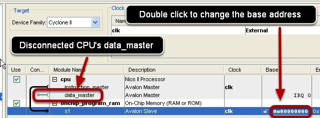
In order to resove some possible errors marked in the mesage section, the base address of the onchip_program_ram need to be changed to 0x00000 as shown in the figure. In the image the disconnected data_master of the CPU can be observed as well.
Add a memory component for data
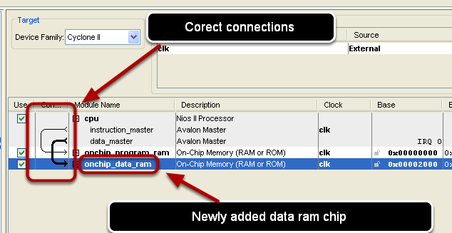
Add a new onchip RAM module, as in a previous step, of 8KB. This new component will ahve a different base address non-overlapping with the previos ram module. If the new ram module's default base address is 0x01000, it will need to be changed, similarly to the case of the program ram, alocating the new chip from the 0x02000 adrress onward. However, in order to use it as a data memory, it will have to be disconnect it from the CPU's instruction_master, in a similar manner the onchip_program_ram from the data_master was disconnected. The new ram chip could also be renamed as in figure
Add other CPU interfaces
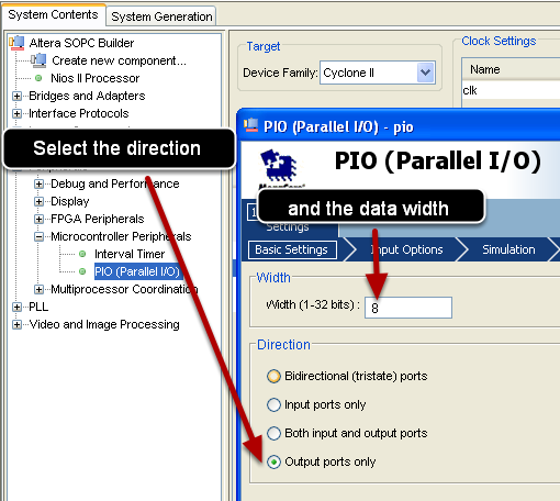
In order to control the LCD of the DE2 board, we will use 3 supplementary interfaces: one for sending data to the LCD, one for specifying the sent data is data or commands and one for starting the communication. All these interfaces will be PIO components as shown in the figure. The first interface, called lcd_data, is an output parallel interfacem with an 8-bit width as displayed in the image. After selecting the data width and dirrection click the Finish button
Add other CPU interfaces cont'd
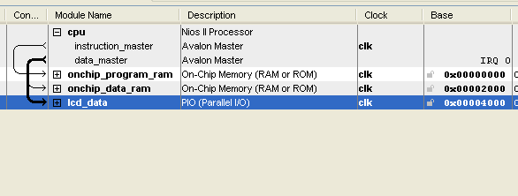
Rename the previously added PIO interface as lcd_data and set its base address to 0x04000 as in the figure. Observe that the newly added interface is by default connected to the data_master of the CPU. This way the CPU will communicate with at least two slaves: one associated with the data memory and another one associated with the lcd_data. The selection of one of them is done dependent of the access address. This is because the Nios II interfaces (such as the lcd_data) are memory mapped, meaning that the data transfers with the components are realized using memory read/write instructions (moreover the interfaces are assigned a base address, with respect to which all communications are realized)
Add other CPU interfaces cont'd
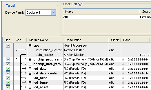
In a similar way add two more output PIO components, of only 1-bit width, one named: lcd_data_cmdn (selecting the transfer of data vs command to the LCD) and another one named lcd_exec, used for issuing the LCD command/data. Additionally, add an input PIO named lcd_busy, which will be checked by the CPU after every LCD operation, to assure the LCD finished the execution. Moreover, imeediately after the activation of the reset signal, the LCD will be busy for at least 20 ms, thus making it necesary for the written program running on the CPU to first check that the initialization sequence of the LCD has finished before attempting any operation with the display. Optionally one can add a supplementary line, allowing to reset the LCD Driver, named lcd_reset, as an output, 1-bit PIO. The mentioned components together with their base addresses are depicted on the figure.
Add other CPU interfaces cont'd
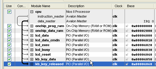
Additional interfaces can be added to the Nios II system, such as, for example, lines form reading characters from a keyboard connected to the DE2's PS/2 port. For this particular scenario, two more PIOs are required, both being inputs (data is read from the Keyboard Driver), one of 8-bit width and another one of only 1-bit width. the module kb_key_data, as depicted in the figure, is used to read the ASCII code of the last released key, while the kb_key_released, become active, for several clock cycles immediately after the key was released. In order to read a key properly, the key_released line must be asserted of value 1, and after the data was read on the key_data lines, the inactive level of key_released will need to be asserted.
Setting the Reset, the Exception and the Break vectors
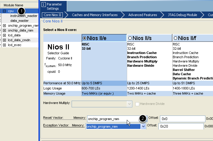
As mentioned in an earlier step, the three vectors need to be set for the nios CPU befor being able to generate the architecture. Double click the cpu component (1) to modify its configuration and select the program ram for the reset vector and the exceptin vector (2). Leave the offset as provided. Similarly in the forth step (the JTAG Debug Module screen) set the program ram as the memory for the Break vector. The Memory selection indicate that immediately after a reset, or after an interrupt is taken or after a debug request is granted by the CPU, its Program Counter is loaded with the address of the routine for treating the respective event, address computed by adding the respective offset to the base address of the memory module selected. Because we do not use interrupts, nor debugging facilities, we can safely set the same offset for the two routines.
Generating the Nios II system
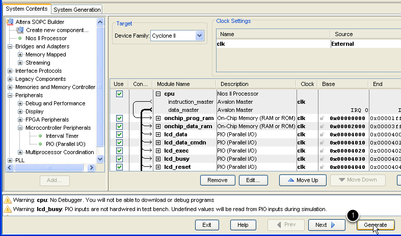
After configuring the system and solving all the errors displayed in the message section, click the Generate button
Adding the Nios II system component on the Block Diagram/Schematic
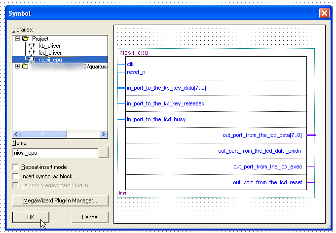
After a successful generation a new symbolis created for the Nios II system, the new component becoming available in the Quartus, as shown in the picture.
Connect the Nios II system to the other components and pins
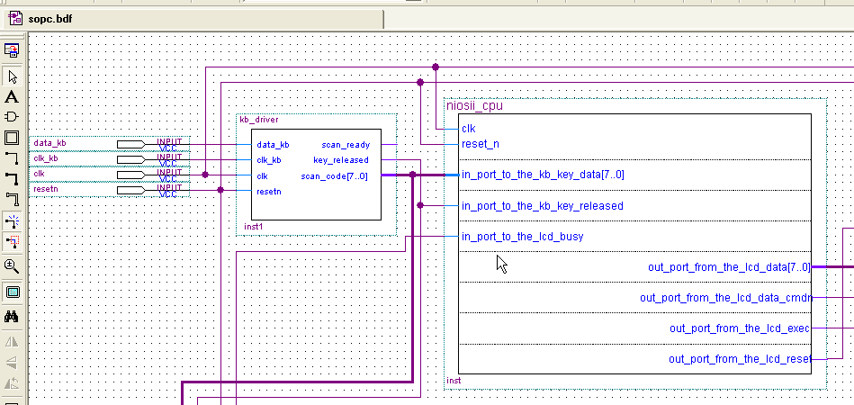
After inserting the CPU system in the design its port are connected to the input/output pins and/or to the other components (LCD Driver for example) as described in the Quartus Project Creation tutorial.